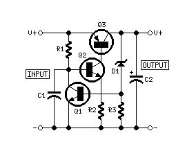
Circuit diagram:
Parts:
R1______________47K  1/4W Resistor
R2_____________120R  1/2W Resistor
R3_____________560R  1/4W Resistor

C1______________68nF  63V Polyester Capacitor
C2_____________220µF  35 or 50V Electrolytic Capacitor (See Text and Notes)

D1__________BZX79C20  20V 1/2W Zener Diode (See Text and Notes)

Q1,Q2__________BC546  65V 100mA NPN Transistors (See Text and Notes)
Q3_____________BD438  45V 4A PNP Transistor (See Text and Notes)
Comments:
This regulated power supply was primarily intended to be employed with audio power amplifiers, namely the 3-5 Watt and 7 Watt Class-A and 18W Class-B but, of course, can be used with a lot of different circuits.
Unlike most dc regulators, the power transistor Q3 is not wired as an Emitter Follower but in the scarcely used Common Emitter configuration instead.
The main advantages of this configuration are: reduced power dissipation in the output transistor and low output voltage drop. This feature means that for obtaining e.g. 20V at the output, a minimum of about 20.5V is required at the input. Using the other configuration, a minimum input of 23V or higher will be necessary in order to obtain the same output voltage as above.
The circuit will work fine in the 5-25V output range and up to 2A by changing only the Zener Diode value (D1).
A single circuit of this kind can therefore be used to power both amplifiers of a stereo unit requiring a single rail supply, like the 3-5W and 7W Class-A Audio Amplifiers.
For dual rail supply designs, like the 18W Class-B Amplifier, two regulators are necessary: the above mentioned circuit for the positive rail and a modified version of the same circuit for the negative one.
Modifications for the negative rail regulator are described in the section below.
Negative Rail Regulator:
The Negative Rail Regulator is identical to the positive type with the exception that all transistor types must be changed whereas D1 and C2 must be reversed in their polarities. Please note that also the output polarity will result reversed in respect to the Circuit diagram.
Parts changed:
Q1,Q2__________BC556  65V 100mA PNP Transistors
Q3_____________BD437  45V 4A NPN Transistor (See Notes)
Notes:
- Q3 power transistor should be mounted on a finned heatsink of about 50x50x25mm.
- To set the output voltage, choose for D1 a Zener Diode having the same voltage required at the output. You can use two Zener Diodes wired in series to obtain uncommon or difficult to locate Zener voltage values.
For example, you can use two 12V Zeners to obtain 24V, or a 10V and a 12V Zener to obtain 22V. - The value of D1 shown in the Parts List is that required to supply the 18W Class-B Amplifier. Modifications required for the Negative Rail Regulator are also suitable for the same amplifier.
- To supply two 3-5W or 7W Class-A amplifiers a single regulator circuit is required, but D1 must be changed to BZX79C24 (24V 1/2W Zener Diode).