Circuit diagram:
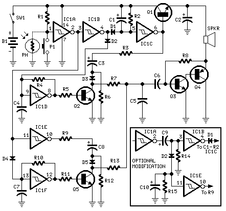
Parts:
R1,R3,R7,R9,R13_10K   1/4W Resistors
R2_______________1M5  1/4W Resistor
R4______________27K   1/4W Resistor
R5,R11__________47K   1/4W Resistors
R6,R12_________220K   1/4W Resistors
R8_______________2M2  1/4W Resistor
R10_____________33K   1/4W Resistor

C1_______________2µ2  25V Electrolytic Capacitor
C2______________47µF  25V Electrolytic Capacitor
C3,C8___________10µF  25V Electrolytic Capacitors
C4,C7___________10nF  63V Polyester Capacitors
C5,C6__________100nF  63V Polyester Capacitors

D1-D5_________1N4148  75V 150mA Diodes

IC1__________MC14106 or 40106 Hex Schmitt Inverter IC

Q1_____________BC337  45V 800mA NPN Transistor
Q2,Q3,Q5_______BC238  25V 100mA NPN Transistors
Q4 ____________BC327  45V 800mA PNP Transistor

PH______________Photo resistor (any type) (see Notes)

P1______________SPST Pushbutton (see Notes)

SW1_____________SPST Switch

SPKR____________8 Ohm Loudspeaker

B1______________3V Battery (two 1.5V AA or AAA cells in series etc.)
Parts added to optional modification:
R14____________220K   1/4W Resistor
R15______________1M   1/4W Resistor

C9_______________4µ7  25V Electrolytic Capacitor
C10______________1µF  25V Electrolytic Capacitor
Device purpose:
This circuit generates a dual-tone bells ringing similar to most door-bell units. It can be used in many applications other than door-bell. In the Notes below several options will be given in order to suit different needs.
Circuit operation:
The circuit as shown in the diagram generates a "Ding-tone" when P1 is pressed and a "Dong-tone" when P1 is released. IC1D is the first-tone frequency generator and IC1F generates the second-tone.
Q2, Q5 and related components act as shape and decay controls of the two tones, trying to imitate as close as possible the bells sound. Their outputs are mixed (R7 & R13), filtered (C5) and boosted by a simple class-A audio amplifier (Q3 & Q4) in order to drive the loudspeaker. The amplifier is switched-on by Q1 when P1 is pressed, then is switched-off some seconds after P1 is released: this time-delay is fixed by C1 & R2. In this way the circuit will draw a negligible current when in stand-by mode.
Notes:
- To obtain a "Ding-Dong" operation when pushing on P1, no matter when it is released, you must modify the circuit as shown in the frame placed at the low-right corner of the circuit diagram. D4 must be removed. C10 & R15 set the time-delay separating first and second tone.
- To obtain a one-tone-only generator, wire the circuit as in the optional modification, making the following changes:
C9 = 100nF 63V Polyester Capacitor.
Omit R9 to R13 & R15; C7, C8 & C10; D2, D4, D5 & Q5.
Connect to negative supply pins 11 & 13 of IC1 and left open pins 10 & 12. - An amusing application of this circuit wired as in the original schematic, is to use a photo-resistor in place of P1, then placing the unit near the flashing lamps of your Christmas tree. A soft bell sound may be heard at switch-on and switch-off of the lamp chosen.
- To obtain higher output power you may substitute R8, Q3 & Q4 with an audio amplifier IC like the LM386 or LM380. In this case power supply must be raised to 6 - 12V but at the same time R4 & R10 should be changed to adjust bell-tone frequencies.
- Good tone frequencies are roughly 2000 and 1650Hz respectively.
- When in stand-by mode, current drawing of the circuit is 200µA @ 3V supply: therefore SW1 can be omitted.