Circuit diagram:
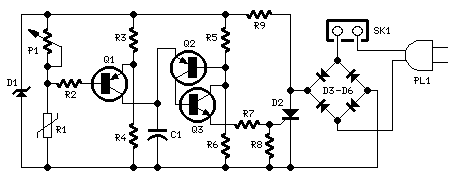
Parts:
P1_____________22K   Linear Potentiometer (See Notes)

R1_____________15K   @ 20°C n.t.c. Thermistor (See Notes)
R2____________100K   1/4W Resistor
R3,R6__________10K   1/4W Resistors
R4,R5__________22K   1/4W Resistors
R7____________100R   1/4W Resistor
R8____________470R   1/4W Resistor
R9_____________33K     4W Resistor

C1_____________10nF   63V Polyester Capacitor

D1________BZX79C18    18V 500mW Zener Diode
D2_________TIC106D   400V 5A SCR
D3-D6_______1N4007  1000V 1A Diodes

Q1,Q2________BC327    45V 800mA PNP Transistors
Q3___________BC337    45V 800mA NPN Transistor

SK1__________Female Mains socket

PL1__________Male Mains plug & cable
Device purpose:
This circuit adopt a rather old design technique as its purpose is to vary the speed of a fan related to temperature with a minimum parts counting and avoiding the use of special-purpose ICs, often difficult to obtain.
Circuit operation:
R3-R4 and P1-R1 are wired as a Wheatstone bridge in which R3-R4 generate a fixed two-thirds-supply "reference" voltage, P1-R1 generate a temperature-sensitive "variable" voltage, and Q1 is used as a bridge balance detector.
P1 is adjusted so that the "reference" and "variable" voltages are equal at a temperature just below the required trigger value, and under this condition Q1 Base and Emitter are at equal voltages and Q1 is cut off. When the R1 temperature goes above this "balance" value the P1-R1 voltage falls below the "reference" value, so Q1 becomes forward biased, pulse-charging C1.
This occurs because the whole circuit is supplied by a 100Hz half-wave voltage obtained from mains supply by means of D3-D6 diode bridge without a smoothing capacitor and fixed to 18V by R9 and Zener diode D1. Therefore the 18V supply of the circuit is not true DC but has a rather trapezoidal shape. C1 provides a variable phase-delay pulse-train related to temperature and synchronous with the mains supply "zero voltage" point of each half cycle, thus producing minimal switching RFI from the SCR. Q2 and Q3 form a trigger device, generating a short pulse suitable to drive the SCR.
Notes:
- The circuit is designed for 230Vac operation. If your ac mains is rated at about 115V, you can change R9 value to 15K 2W. No other changes are required.
- Circuit operation can be reversed, i.e. the fan increases its speed as temperature decreases, by simply transposing R1 and P1 positions. This mode of operation is useful in controlling a hot air flux, e.g. using heaters.
- Thermistor value is not critical: I tried also 10K and 22K with good results.
- In this circuit, if R1 and Q1 are not mounted in the same environment, the precise trigger points are subject to slight variation with changes in Q1 temperature, due to the temperature dependence of its Base-Emitter junction characteristics. This circuit is thus not suitable for use in precision applications, unless Q1 and R1 operate at equal temperatures.
- The temperature / speed-increase ratio can be varied changing C1 value. The lower the C1 value the steeper the temperature / speed-increase ratio curve and vice-versa.
- Warning! The circuit is connected to 230Vac mains, then some parts in the circuit board are subjected to lethal potential! Avoid touching the circuit when plugged and enclose it in a plastic box.