Circuit diagram:
Parts:
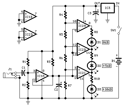
R1_____________300K  1/4W Resistor
R2_______________1M2 1/4W Resistor
R3_____________510K  1/4W Resistor
R4_____________220K  1/4W Resistor
R5______________91K  1/4W Resistor
R6_____________160K  1/4W Resistor
R7______________56K  1/4W Resistor
R8,R9__________100R  1/4W Resistors
R10____________220R  1/4W Resistor

C1_____________100nF  63V Polyester Capacitor
C2_______________1µF  63V Polyester or Electrolytic Capacitor
C3______________10µF  25V Electrolytic Capacitor

D1,D2,D3_________3mm  LEDs (Any coloring at will)

IC1____________LM393  Dual Comparator IC
IC2____________LM324  Low power Quad Op-Amp IC
IC3____________78L05  5V 100mA Regulator IC

J1_____________6.3mm  Mono Jack socket

SW1_____________SPST  Toggle or Slider Switch

B1________________9V  PP3 Battery

Clip for PP3 Battery
Comments:
This circuit was designed to provide a valuable test equipment tool for sound reinforcement systems like guitar amplifiers and the like. Used in conjunction with a signal generator it can be of considerable help in setting and controlling levels through any amplifying chain.
Please see the Spot-frequency Sine wave Generator or 1KHz Sine wave Generator designs, all available on this website, to complete the equipment.
The circuit is formed by an input buffer and ac to dc voltage converter (IC1A) feeding a window comparator (IC2A, IC2B, IC2C) which illuminates one of three LEDs at a time.
No setup is required: if correct values are used for resistors R3 to R7, LED D1 will illuminate at 0dB input (0.775V RMS), LED D2 at +5dB input (1.378V RMS) and LED D3 at +10dB (2.451V RMS).
The circuit was optimized for low current consumption as it was intended for battery operation. To achieve this, the best arrangement has proven to be the one using two different op-amp types for IC1 and IC2. In fact the LM393 IC was not operating satisfactorily as dot-mode LED driver, whereas the LM324 was unable to charge C2 in the linear way, as expected. Therefore, the final circuit is some op-amp wasting, but the small added cost will be quickly compensated by battery savings.
Notes:
- Maximum current drawing: 12mA when one of the three LEDs is illuminated and less than 4.5mA when the input level is below 0.775V.
- The 5V dc regulator IC (IC3) is required to greatly improve circuit precision.
- 2% or 1% tolerance preferred for resistors R3 to R7.
- LEDs of different colors can be used to mark any of the three different levels.
- Input pins of unused op-amps must be tied to negative ground. Output pins must be left open (see the upper left corner of the drawing).